


Infineon Technologies CoolGaN™ G3 Transistors

Infineon Technologies CoolGaN™ G3 Transistors are designed to deliver superior performance in high-power density applications. These transistors feature a very low on-state resistance, enabling efficient power conversion and reduced energy losses. Available in four voltage options (60V, 80V, 100V, or 120V), the Infineon CoolGaN G3 Transistors deliver ultra-fast switching with an ultra-low gate/output charge. The transistors are housed in compact PQFN packages, which enhance thermal management and support dual-side cooling, ensuring reliable operation even under demanding conditions. These features make CoolGaN G3 Transistors a top choice for applications such as telecom, data center power supplies, and industrial power systems.
Features
- Ultra-fast switching and high efficiency
- Space-saving and highly robust package
- No reverse recovery charge
- Ultra-low gate and output charge
- Exposed die for top‑side thermal excellence
- Moisture Sensitivity Level (MSL) 1
- Industrial grade 3mm x 5mm PG‑TSON‑6 package
- Fully qualified according to JEDEC for industrial applications
- Lead-free, Halogen-free, and RoHS-compliant
Applications
- Battery-powered tools
- e‑Mobility and UAVs
- Robotics and drones
- Solar and energy storage systems
- Telecom and data centers
- Low‑power SMPS
- Sync rectification for AC‑DC and DC‑DC converters
Specifications
- 60V, 80V, 100V, or 120V maximum continuous drain‑source voltage
- 45W maximum power dissipation
- ±6.5V maximum pulsed gate‑source voltage
- -4.0V to 5.5V gate source voltage range
- 1.2V to 2.9V gate threshold voltage range
- 0.5Ω typical gate resistance
- 1.9mΩ to 3.7mΩ maximum drain‑source on‑state resistance range
- Capacitance
- 1100pF to 1700pF maximum input range
- 550pF to 770pF maximum outputrange
- 6.4pF to 22pF maximum reverse transfer range
- Typical gate charge
- 2.7nC to 4.0nC gate-to-source charge range
- 2.9nC to 2.0nC gate charge at threshold range
- 2.3nC to 3.6nC gate-to-drain charge range
- 3.0nC to 4.7nC switching charge range
- 10nC to 13nC gate charge total range
- 2.7V to 2.8V gate plateau voltage range
- 37nC to 49nC output charge range
- Reverse operation
- 15A to 16A maximum reverse continuous current range
- 284A to 396A maximum reverse pulsed current range
- 3.4V maximum source-to-drain voltage
- 0nC typical reverse recovery charge
- -40°C to +150°C junction temperature range
- Thermal resistance
- 0.6°C/W maximum junction-to-case top
- 2.8°C/W maximum junction-to-case bottom
- 60°C/W typical junction-to-ambient 1s0p
- 38°C/W typical junction-to-ambient 2s2p
Dimensions

Related Transistors

Infineon Technologies CoolGaN™ 100V G3 Transistors
Normally OFF, enhancement-mode (e-mode) power transistor in a compact housing.
Development Tool
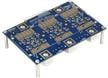
Infineon Technologies EVAL_MTR_48V150A_GaN Evaluation Board
Designed to showcase the capabilities of CoolGaN™ 80V G3 transistors in high‑current applications.
Related Application

Infineon Technologies GaN-Based Motor Control for Humanoid Robots
Engineered for maximum performance, compact design, and superior energy efficiency.
| N.º de artículo | Hoja de datos | Descripción |
|---|---|---|
| IGC037S12S1XTMA1 |  |
GaN FETs CoolGaN Transistor 120 V G3 in PQFN 3x5, 2.7 mohm |
| IGB070S10S1XTMA1 | |
GaN FETs CoolGaN Transistor 100 V G3 in PQFN 3x3, 5 mohm |
| IGB110S10S1XTMA1 | |
GaN FETs CoolGaN Transistor 100 V G3 in PQFN 3x3, 9.4 mohm |
| IGC019S06S1XTMA1 | |
GaN FETs CoolGaN Transistor 60 V G3 in PQFN 3x5, 1.3 mohm |
| IGC025S08S1XTMA1 | |
GaN FETs CoolGaN Transistor 80 V G3 in PQFN 3x5, 1.8 mohm |
| IGB110S101XTMA1 | |
GaN FETs MV GAN DISCRETES |
| IGC033S101XTMA1 | |
GaN FETs MV GAN DISCRETES |
| IGC033S10S1XTMA1 | |
GaN FETs MV GAN DISCRETES |