



Microchip Technology dsPIC33AK MPS Digital Signal Controllers (DSCs)

Microchip Technology dsPIC33AK MPS Digital Signal Controllers (DSCs) combine a 200MHz 32-bit dsPIC33A core with single- and double-precision floating-point processing for high-performance real-time control. These devices integrate up to 256KB Flash memory, 64KB SRAM, and advanced digital signal processing capabilities. Designed for precision sensing and control, the dsPIC33AK MPS family features high-speed 12-bit Analog-to-Digital Controllers (ADCs) operating at up to 40Msps, integrated op-amps, fast comparators, and high-resolution Pulse Width Modulation (PWM) outputs. Advanced peripherals support digital power, industrial automation, sensing, touch control, and other demanding embedded applications.
The Microchip Technology devices also incorporate functional safety and security features, including secure boot, cryptographic acceleration, error-correcting memory, and post-quantum cryptography support. Compliance-ready designs help accelerate the development of safety-critical and industrial systems that require reliable operation and robust protection.
Features
- Operating conditions
- 3.0V to 3.6V: -40°C to +85°C, DC to 200MHz
- 3.0V to 3.6V: -40°C to +125°C, DC to 200MHz planned
- 3.0V to 3.6V: -40°C to +150°C, DC to 200MHz planned
- High-performance DSP CPU
- 32-bit rich instruction set for optimized speed and program code size
- 16-bit dsPIC33 core compatible
- Non-paged linear data/Flash 24-bit addressing space
- 16-bit/32-bit instructions for optimized code size and performance
- 32-bit wide data paths
- Single and double precision Floating-Point Unit (FPU) coprocessor
- 2kbyte instruction cache
- Sixteen 32-bit working registers
- Dual 72-bit accumulators supporting 32-bit and 16-bit fixed-point DSP operations
- Eight-level deep working register sets
- Eight-level deep accumulator register sets
- Eight-level deep floating-point register sets
- 32-bit rich instruction set for optimized speed and program code size
- Memory
- Up to 256Kbytes of program Flash memory
- 10,000 erase/write cycle endurance
- 20 years minimum data retention
- Self-programmable under software control
- Programmable code protection
- Flash Error Correcting Code (ECC)
- Dual Flash panel
- Live update support
- Programmable OTP regions
- Entire Flash OTP by ICSP™ write inhibit
- Separate 64x128-bit OTP
- Up to 64Kbytes of static RAM
- RAM Error Correcting Code (ECC)
- RAM Memory Built-In Self-Test (MBIST)
- Up to 256Kbytes of program Flash memory
- Security
- Flash OTP by ICSP write inhibit - on-chip secure boot Flash configurable as an immutable Root of Trust, with parts of the Flash memory that can be configured as OTP
- Capabilities include
- Secure boot support with validation of the host code image and the host code signature
- Secure update support for host code: Secure encryption key storage and image decryption
- X.509 certification storage, parsing, validation, and revocation, supporting both ECC and RSA
- 128-bit Unique Device Serial Number for Identification (UUID)
- Support for secure use cases
- Secure boot
- Key storage in the IRT/immutable secure boot region for realizing
- Secure boot
- Secure firmware update
- Secure debug
- Flash protection
- Configuration of up to eight Flash protection regions across ranges of Flash addresses
- Regions can be configured as
- Immutable Root of Trust (IRT)
- OTP region
- A combination of R/W/X protections
- Regions can be
- Made permanent
- Locked until device reset
- Enabled/disabled during code execution
- Flash protection regions can apply to the active partition, the inactive partition, or both
- Crypto accelerator module (CAM) - AES-128, AES-192, and AES-256 (fully compliant with NIST FIPS 197); ECB, CBC, CFB, OFB, CTR, GCM, CCM, XTS, CMAC modes
- HASH/MAC
- SHA3-224, SHA3-256, SHA3-384, SHA3-512, SHAKE128 and SHAKE256 capability
- SHA-1, SHA-256, SHA-224, SHA-384 and SHA-512 capability
- Public key cryptography with RSA, DSA, and ECC
- RSA with/without Chinese Remainder Theorem (CRT) and up to 4096-bit key length
- Prime Field P-192, P-224, P-256, P-384, P-521
- Binary Field K-163, K-233, K-283, K-409, K-571
- Binary Field B-163, B-233, B-283, B-409, B-571
- P-224, P-256, P-384, and P-521 elliptic curve – ECDSA sign/verify
- DSA support for up to 2048-bit key length
- ECDH support for P256 and P224 curves
- SECP256K1 (bitcoin/blockchain curve) ECDSA support
- 256-bit Brainpool elliptic curve support – ECDSA, ECDH
- Elliptic curve Diffie-Hellman (ECDH/ECDHE) key agreement
- RSA with/without Chinese Remainder Theorem (CRT) and up to 4096-bit key length
- NIST-800-22 and NIST-800-90B compliant True Random Number Generator (TRNG)
- High-resolution PWM
- Multiple PWM generators with four pairs (eight outputs) generators, with Fine Edge Placement (FEP) resolution down to 78ps
- Dead time for rising and falling edges
- Dead-time compensation supports lower speed operation
- Clock chopping for high-frequency operation
- PWM support for
- BLDC, PMSM, ACIM, SRM, and stepper motors
- Constant on-time, hysteretic, burst-mode power applications
- Fault and current limit inputs
- Flexible trigger configuration for ADC triggering
- High-speed analog-to-digital Converters
- Three 12-bit resolution SAR ADCs
- Up to 40Msps conversion rate per ADC
- Up to 14 analog input pins
- 16-bit sampling capability
- Sixteen settings channels, where each channel can
- Be assigned to any analog input (I/O pin or internal signal)
- Be set to a different sampling time
- Be configured as single-ended or differential
- The conversion result can be formatted as unsigned or signed
- The conversion result can be left-aligned (fraction format)
- Has a separate 32-bit conversion result register
- Supports four sampling modes
- Oversampling of multiple samples
- Integration of multiple samples
- Window (multiple samples accumulated when the gate signal is active)
- Single conversion
- All channels have a digital comparator to detect configurable thresholds
- The last three setting channels have the second result accumulator to implement second-order filters
- Peripherals
- Three 4-wire SPI modules (up to 50Mbps)
- 32-byte FIFO
- Variable data width
- I2S mode
- Multi-channel digital audio interfaces (I2S)
- Three 16-bit resolution capable audio-rate ADCs at 156kSPS
- DMA-enabled real-time audio streaming (eight DMA channels available)
- TDM4/8/16/32 capable using framed SPI mode with DMA peripheral
- Audio DSP for voice and acoustic processing
- Two I2C modules w/address masking and IPMI support
- One I3C module w/primary and secondary controller modes, and I3C/I2C target capability
- Four protocol UARTs with 8-character RX/TX FIFOs and automated handling support for
- LIN 2.2
- DMX
- Smart card (ISO 7816)
- IrDA®
- Two SENT modules
- Three dedicated 32-bit timer/counter modules
- Output capture/compare/PWM/timer modules
- One MCCP
- Four SCCPs
- Flexible configuration as PWM, input capture, output compare, or timers
- Two 16-bit timers or one 32-bit timer in each module
- 8-channel hardware Direct Memory Access (DMA) module
- One Quadrature Encoder Interface (QEI) module with four inputs (Phase A, Phase B, Home, and Index)
- Serial encoder interface BiSS with support for up to four client encoders
- Four Configurable Logic Cells (CLC) with internal connections to select peripherals and PPS
- Peripheral Trigger Generator (PTG)
- 16 possible trigger sources to other peripheral modules
- CPU-independent state machine-based instruction sequencer
- One CAN FD module
- Integrated Touch Controller (ITC) module
- Advanced capacitive sensing, touch buttons, sliders, and wheels
- Up to 24 self-capacitance and up to 72 mutual-capacitance channels
- One Resolver-to-Digital Converter (RDC) module
- Three 4-wire SPI modules (up to 50Mbps)
- Controller
- High-current I/O sink/source
- Programmable weak pull-up and pull-down resistors
- Programmable open-drain outputs
- Edge or level change notification interrupt on I/O pins
- Peripheral Pin Select (PPS) remappable pins to reduce board layout complexity
- Multiple interrupt vectors with individual programmable priority
- Five external interrupt pins
- Selectable oscillator options, including
- 8MHz, 1% at 0ºC to 85ºC internal Fast RC (FRC) oscillator
- 8MHz, 2% internal Backup Fast RC (BFRC) oscillator with 32kHz divided output
- High-speed crystal resonator oscillator or external clock
- Two 1.6GHz PLLs, which can be clocked from the FRC or a crystal oscillator
- Reference clock output (REFO)
- Low-power management modes (sleep and idle)
- Power-on reset and brown-out reset
- On-board 1.1V Buck voltage regulator for core voltage supply
- Analog
- Up to five 5nS analog comparators with 12-bit PDM DACs
- Input multiplexing
- Slope compensation
- Up to two DAC output buffers
- Three rail-to-rail 100MHz operational amplifiers with
- 40V/μS slew rate
- 1mV offset (typ.) with calibration feature
- VREF/2 output available for op amp input biasing
- Four 10µA constant-current sources, four programmable current sources
- Integrated touch controller
- Independent of ADC processing capability
- Self and mutual CVD touch modes support
- 11 to 24 touch ADC RX inputs
- 9 to 15 touch TX outputs
- Up to five 5nS analog comparators with 12-bit PDM DACs
- Safety
- Windowed Watchdog Timer (WDT)
- Deadman Timer (DMT)
- Eight I/O Integrity Monitors (IOIM)
- Fail-Safe Clock Monitor (FSCM) with automatic switchover to backup clock source, featuring programmable over-frequency/under-frequency thresholds
- Flash Error Correcting Code (ECC)
- RAM Error Correcting Code (ECC)
- RAM Memory Built-In Self-Test (MBIST)
- 32-Bit Cyclic Redundancy Check (CRC) module
- Entire Flash OTP by ICSP write inhibit
- Internal voltage regulators
- Virtual PPS pins for redundancy and monitoring
- Temperature sensor diode
- Power monitor for core voltage with configurable fault injection
- Functional safety
- Targets
- ISO 26262 ASIL B
- IEC 61508 SIL 2
- IEC 60730 Class B
- ISO 26262 and IEC 61508 compliant device development
- Targets
Applications
- Power Factor Correction (PFC)
- Interleaved PFC, totem-pole PFC
- Critical conduction PFC
- Multi-level flying capacitor PFC
- DC-DC converters
- Buck, Boost, Forward, Flyback, Push-Pull
- Half-/full-bridge
- Phase-shift full-bridge
- Resonant converters
- DC-AC
- Half-/full-bridge inverter
- Resonant inverter
- Motor control
- BLDC
- PMSM
- SR
- ACIM
- Advanced sensor interfacing
- High-performance embedded control
- High-speed data acquisition and processing
- Safety-critical designs
- Digital lighting
Block Diagram

Core Block Diagram

Related DSCs
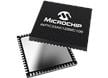
Microchip Technology dsPIC33AK Digital Signal Controllers (DSCs)
Designed for high-performance and real-time precision control applications.
Development Tools

Microchip Technology EV17P63A Curiosity Nano Evaluation Kit
A cost-effective board that facilitates easy evaluation and adoption of 32-bit dsPIC33A DSCs.

Microchip Technology dsPIC33AK256MPS306 General Purpose DIM (EV02E57A)
Demonstrates the capabilities of the dsPIC33AK256MPS306 family of Digital Signal Controllers (DSCs).

Microchip Technology dsPIC33AK256MPS306 Motor Control DIM (EV22K90A)
Used to evaluate the entire dsPIC33AK256MPS306 DSC family for motor control applications.

Microchip Technology dsPIC33AK512MPS506 Digital Power PIM
Showcases the dsPIC33AK512MPS506 Digital Signal Controller (DSC) features.

Microchip Technology Depurador/programador en circuito MPLAB® PICkit™ 5
Permite crear prototipos rápidos listos para producción portátil para todos los componentes de Microchip.

Microchip Technology Depurador básico MPLAB® Pickit™
Ideal for projects not requiring high-voltage programming or advanced debug features.

Microchip Technology dsPIC33A Digital Power Starter Kit 4
Digital power kit with buck and boost stages, onboard loads, programming, and debugging.